
|
| Email Home Page |
|
|
|
|
| Email Home Page |
|
|
|
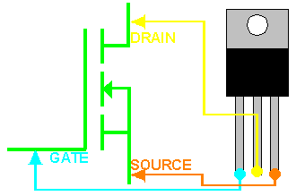
The function of Field Effect Transistors is similar to bipolar transistors (especially the type we will discuss here) but there are a few differences. They have 3 terminals as shown below. Two general types of FETs are the 'N' channel and the 'P' channel MOSFETs. Here we will only discuss the N channel. Actually, in this section, we'll only be discussing the most commonly used enhancement mode N channel MOSFET (Metal Oxide Semiconductor Field Effect Transistor). Its schematic symbol is below. The arrows show how the LEGS of the actual transistor correspond to the schematic symbol.
Current Control: When FETs are used in the audio output section of an amplifier, the Vgs (voltage from gate to source) is rarely higher than 3.5 volts. When FETs are used in switching power supplies, the Vgs is usually much higher (10 to 15 volts). When the gate voltage is above approximately 5 volts, it becomes more efficient (which means less voltage drop across the FET and therefore less power dissipation). MOSFETs are commonly used because they are easier to drive in high current applications (such as the switching power supplies found in car audio amplifiers). If a bipolar transistor is used, a fraction of the collector/emitter current must flow through the base junction. In high current situations where there is significant collector/emitter current, the base current may be significant. FETs can be driven by very little current (compared to the bipolar transistors). The only current that flows from the drive circuit is the current that flows due to the capacitance. As you already know, when DC is applied to a capacitor, there is an initial surge then the current flow stops. When the gate of an FET is driven with a high frequency signal, the drive circuit essentially sees only a small value capacitor. For low to intermediate frequencies, the drive circuit has to deliver little current. At very high frequencies or when many FETs are being driven, the drive circuit must be able to deliver more current.
Note:
High Current Terminals:
Transistor Packages:
Transistor In Circuit:
----- Critically Important -----
Adobe has deemed that the Flash content on web pages is too risky to be used by the general internet user. For virtually all modern browsers, support for Flash was eliminated on 1-1-2021. This means that those browsers will not display any of the interactive Flash demos/calculators/graphics on this (or any other) site.
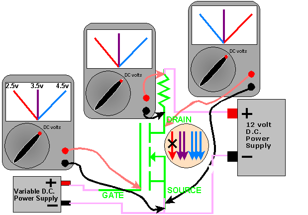
The simplest (not the best) fix, for now, is to download the Ruffle extension for your browser. It will render the Flash files where they were previously blocked. In some browsers, you will have to click on the big 'play' button to make the Flash applets/graphics visible. An alternative to Ruffle for viewing Flash content is to use an alternative browser like the older, portable version of Chrome (chromium), an older version of Safari for Windows or one of several other browsers. More information on Flash capable browsers can be found HERE. It's not quite as simple as Ruffle but anyone even moderately familiar with the Windows Control Panel and installation of software can use Flash as it was intended. In the following demo, you can see that there is an FET connected to a lamp. When the voltage is below about 3 volts, the lamp is completely off. There is no current flowing through the lamp or the FET. When you push the button, you can see that the capacitor starts to charge (indicated by the rising yellow line and by the point where the capacitor's charging curve intersects with the white line sweeping from left to right. When the FET starts to turn on, the voltage on the drain starts to fall (indicated by the falling green line and the point where the green curve intersects with the white line). As the gate voltage approaches the threshold voltage (~3.5v), the voltage across the lamp starts to increase. The more it increases, the brighter the lamp becomes. After the voltage on the gate reaches about 4 volts, you can see that the bulb is fully on (it has the full 12 volts across its terminals). There is virtually no voltage across the FET. You should notice that the FET is fully off below 3 volts and fully on after 4 volts. Any gate voltage below 3 volts has virtually no effect on the FET. Above 4 volts, there is little effect.
Gate Voltage:
Current:
Voltage:
Power Dissipation: |
|

|
|

|