
|
| Email Home Page |
|
|
|
|
| Email Home Page |
|
|
|
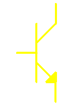
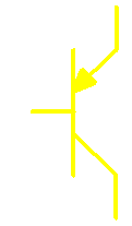
This section will, in no way, tell you everything about transistors. It will just give you a general idea what transistors are and how they may be used in car audio. The two main types of transistors are bipolar transistors and field effect transistors. A bipolar transistor uses a small current to control a larger current, a little like a relay. Bipolar transistors generally have 3 terminals. The control terminal is called the base. The other 2 terminals are known as the emitter and the collector and they carry virtually all of the current flowing through the transistor. There are 2 basic configurations of bipolar transistors, one is an 'NPN' the other is a 'PNP'. The two are very similar. The biggest difference is the direction of current flow through the collector and emitter. For now we will mainly discuss the NPN transistor.
Current Control:
One problem faced by installers is the need to reliably switch a relay when the switching output from the control device is less than the 12 volts needed to actuate the relay. In the first diagram, you can see that the voltage applied to the resistor is 0v D.C. and the relay contacts are not closed. In the next diagram, you will see that 12 volts D.C. is applied to the resistor and the relay contacts are closed (because the transistor is now conducting current).
You no doubt noticed the resistor connected to the base of the transistor. This is to prevent damage to the transistor. If the voltage applied to the base is greater than approximately .6 volts (with respect to the emitter) the transistor may be damaged. Think of it like this... (I know my analogies ARE lame, but they will help some people) If you were turning a light switch on with the blade on the front of a bulldozer (don't try this at home, kids), you would have to be very precise in positioning the blade to prevent damaging the switch. If you connected the switch to the dozer blade with a rubber band, the dozer blade could still turn on the switch and the blade could go as high as physically possible without destroying the switch. Now, what if the rubber band is too strong or too weak? The switch might still be destroyed if the rubber band was too strong or, if the rubber band is too weak, the switch may not be switched 'on' at all (even at the highest position of the dozer blade). The same is true with the transistor. If a resistor with a low resistance is connected in series with the base and a high voltage is applied to the resistor, the transistor may still be destroyed. If the resistor has a very high resistance and a voltage is applied to it, the transistor may not be fully turned on. If a transistor is only partially turned on, it means that there will be a voltage drop between the collector and the emitter of the transistor and the transistor may become hot. If a transistor is connected as shown in the previous diagram, there will be a voltage drop across it because the transistor cannot be turned 'on' enough to have absolutely no voltage across it while current is flowing through it. Since there is a voltage drop across the transistor and current flowing through it, there will be power dissipation in the form of heat. The amount of heat produced is determined by the power dissipation. If the transistor is not mounted to a heat sink, it may be destroyed by the heat.
Now, just for fun, push, pull or drag your mouse over the image below. Watch the voltmeter and the relay's movable contact.
Design Parameters:
Beta:
Current:
Voltage:
Power Dissipation:
 B=base C=collector E=emitter
This photo shows you the difference in size between the actual piece of silicon and the size of the package. It shows that the silicon is significantly smaller than the package it's in. This is an MJE15030. The body of this transistor measures approximately 0.6" x 0.4". The silicone die inside the package is approximately 0.11" square.

 |
|

|
|

|