Factors that Cause an Amplifier to Fail Prematurely
Amplifier Failure:
One of the main reasons that amplifiers fail is improper speaker connection. If too many speakers are connected to an amplifier, the amplifier will be more likely to fail. This section will help you to understand why too many speakers will cause an amplifier to fail. This page applies, primarily, to linear type amplifiers (class A, B and AB amplifiers, not class D, class T or other switching type amplifiers).
----- Critically Important -----
Flash graphics viewing/use alternatives:
Flash support by most modern browsers has been dropped but that's not the end of the line for Flash.
There is no practical alternative to Flash for the interactive demos/applets/graphics on this site.. Especially when there are alternatives, some simple, some good, some...
Ruffle is chosen by most because they can't imagine using anything but their preferred browser. It works. It's OK but not great. The Flash graphics won't look as they're supposed to but it, generally, works.
The #1 preferred (by me) way to view the site and the Flash graphics is with the Chromium Portable browser and the installation of the older (no time-out) Flash Player files. This was incredibly simple when people knew computers but not today when people only know how to work with their phones.
The Flash Browser is a good option but it's so stripped down that it makes it somewhat difficult to use.
The Maxthon browsers are an option. The v4.95 is the easiest (install and use). V5.3.8 and 6.1.0 require (very) slightly more effort (very).
The Chromium and Maxthon browsers on the page above are 'portable' browsers. They are not installed into your system. They are simply made available for use on your computer. They can be carried around on a Flash drive and used on any computer.
----- Critically Important -----
Output Basics:
The diagram below shows a few parts of an amplifier. You will notice that the amplifier has a power supply which produces output voltages of (+)35 volts DC and (-)35 volts DC. The +35 volts is the supply voltage for the PNP bipolar transistor labeled 'transistor A'. Anytime that the output voltage of the amplifier (to the speaker) is a positive voltage, the PNP transistor will allow the proper amount of current to flow from the +35v supply. When the output voltage is negative, the NPN transistor will allow the proper amount of current to flow from the -35v supply.
The voltage at all points along the sine wave are the instantaneous voltages applied to the speaker.
When you come across the power dissipation figures, keep in mind that 35 watts is enough power dissipation to keep a soldering iron at more than 700 degrees fahrenheit.
Output Voltage at Point "A":
At point A, the output voltage is 0 volts. The speaker would be at its point of rest. There would be no current flowing through the output transistors (except a small amount of bias current). There is virtually no power dissipation at this point. In the following calculations:
Psp is the power dissipation in the speaker's voice coil.
Ptr is the power dissipation in the transistor.
Psp = E²/R
Psp = 0²/4
Psp = 0 watts
Ptr = I*E
Ptr = 0*35
Ptr = 0 watts
Output Voltage at Point "B":
At point B, the output voltage of the amplifier is essentially the same as the supply voltage. The voltage across the PNP transistor is approximately 0 volts (it is fully turned on). The current flowing through the PNP transistor is as high as it can be with the current speaker load (lets assume that it is a 4 ohm speaker). Since we know that we have a 4 ohm speaker and 35 volts applied to it, we know (for this point in time):
the current passing through the PNP transistor to the speaker is 8.75 amps (I=E/R). There is virtually no power dissipation across the PNP transistor. There is no current flowing through the NPN transistor. If you could take a 'snap shot' of the speaker at this point in time, the speaker would be pushed OUT as far out as the amplifier is able.
Itotal = V/R
Itotal = 35/4
Itotal = 8.75 amps
Psp = E²/R
Psp = 35²/4
Psp = ~306 watts
Ptr = I*E
Ptr = 8.75*0
Ptr = 0 watts
If the speaker load is 2 ohms, the current flowing through the PNP transistor would double to 17.5 amps. The power dissipation in the PNP transistor would not increase significantly because the voltage across it is very small.
Output Voltage at Point "C":
At point C, the output voltage of the amplifier is below the reference which means that the voltage is negative (with respect to the reference). The output voltage is approximately -15 volts. This means that the voltage across the NPN transistor is 20 volts (the supply voltage - the output voltage). The current through the speaker AND the NPN transistor is 3.75 amps. The power dissipation in the speaker is 56.25 watts (P=I*E). The power dissipation in the transistor is 75 watts. There is no current flowing in the PNP transistor. A snap shot of the speaker at this point would show the speaker pulled IN approximately 1/2 as far as the amplifier is able.
Itotal = V/R
Itotal = 15/4
Itotal = 3.75 amps
Psp = I*E
Psp = 3.75*15
Psp = 56.25 watts
Ptr = I*E
Ptr = 3.75*20
Ptr = 75 watts
A 2 ohm load would result in 150 watts being dissipated in the NPN transistor (twice the power caused by the 4 ohm load).
Output Voltage at Point "D":
At point D, The output voltage of the amplifier is approximately +20 volts. This means that the voltage across the PNP transistor is 15 volts. We know that 20 volts is applied to the 4 ohm speaker. This means that the current through the speaker AND the PNP transistor is 5 amps. This tells us that the power dissipation across the speaker is 100 watts. The PNP transistor is dissipating 75 watts. There is no current flowing through the NPN transistor.
Itotal = V/R
Itotal = 20/4
Itotal = 5 amps
Psp = I*E
Psp = 5*20
Psp = 100 watts
Ptr = I*E
Ptr = 5*15
Ptr = 75 watts
A 2 ohm speaker load would cause the current to double to 10 amps. Since the PNP transistor has 15 volts across it, the power dissipation would be 150 watts.
From this and earlier pages, you should remember:
Power dissipation in any device causes a rise in temperature of the device.
As temperature rises in transistors (and virtually any other electronic device), they are less able to withstand stress. Under adverse conditions, they are more likely to fail when hot.
All else being constant, lowering the impedance of the load on the amplifier will cause the output current to increase.
Bridging a speaker onto an amplifier doubles the voltage across the speaker (compared to the non-bridged connection)
When you double the voltage across a given load the current through the load doubles.
The current driven into the speaker is supplied by the output transistors.
If the current driven into the speaker load is doubled (by bridging) then the current through the output transistors is doubled which increases the power dissipated by the transistor by a factor of 4.
From the above statements, you should be able to see that bridging an amplifier into a load with a lower impedance than recommended will very quickly push an amplifiers components past their design limits.
Checking Field Effect Transistors (MOSFETs)
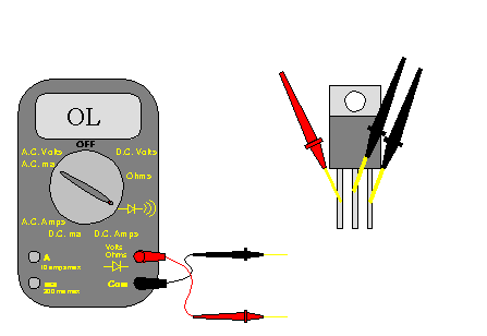
The following diagrams will show you how to check an FET to see if it is bad. This is only for N channel enhancement mode FETs (the type used in most amplifiers' power supplies). Since I use Fluke meters exclusively, all measurements will show what you would see with a Fluke meter. Other digital meters should give very similar readings. Until you become extremely familiar with FETs, you should check the FET in this order from top to bottom. If the order is changed, you may not get accurate test results. To check P-channel FETs, you will need to reverse the meter leads.
This image is checking to see if the gate is leaking or shorted. In this type of FET, the gate should be COMPLETELY isolated from the other two terminals when checking the transistor with a volt meter. During this first test, you are inadvertently charging the gate and turning the transistor on. The meter should read the same as if the leads are open (not touching anything). You should notice that there are two black leads. this means that you first check the transistor with the red lead on the first leg and the black lead on the second leg. Then you move the black lead to the third leg of the transistor (while leaving the red lead on the first leg). The readings should be the same in both positions. The meter is set to its 'diode check' position.
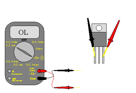
In this image, you are discharging the gate and making sure that the transistor is turned off for the next test. The meter should again read the same as if the leads are open (not touching anything). If it gives any other reading, the transistor is bad.
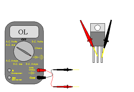
In this image, you're checking to see if there is any leakage between the drain and the source. The meter should again show no continuity between the drain and the source.
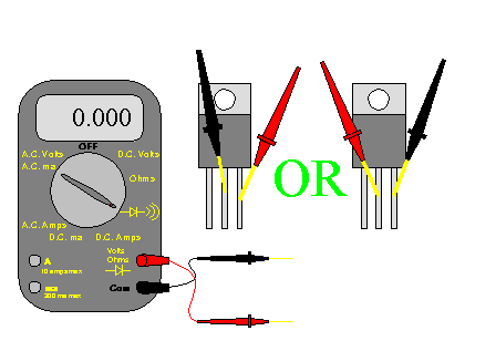
In this image, your meter should read approximately 0.4 to 0.5 volts on diode check (the same meter setting as the previous tests). Here the meter is showing the forward voltage of the intrinsic diode of the FET.
If you get any reading other than 'open' on the first 3 tests, the transistor is defective. If the readings on the last test is below approximately 0.4 volts, the transistor is likely defective. If it reads around 0.3 volts or lower, the FET is definitely defective. The transistor is bad in both of these examples. It shows that the drain and source are shorted together.
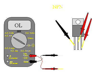
Checking Bipolar Junction Transistors
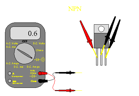
This type of transistor is used throughout all types of electronic equipment. To check PNP transistors, reverse the positions of the red and black leads.
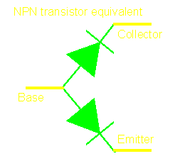
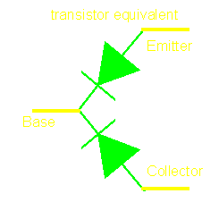
This is a close approximation of the junctions in both NPN and PNP bipolar transistor. I included it to help you to remember how/why the following tests are done.
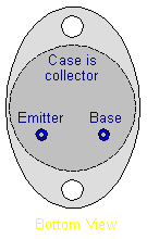
This is the pin out configuration of a TO-3 transistor. The test procedure is the same as the bipolar transistor in the next diagram. Take note of the pins labeled on the diagram for the TO-220 case transistor.
In this diagram, the volt meter applies a small voltage to the transistor's junctions. With the leads in this position, the junctions are forward biased. The reading should be between 0.5 and 0.7 volts. Readings outside this range are likely defective.
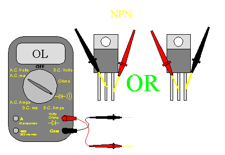
In this diagram, the junctions are being checked with reverse bias. No current should flow through the transistor's junctions with the leads in this position. The meter reading should be the same as it would read with open leads.
Both of these connections should also read as open. any other readings indicate defective transistors. The only exception will be with darlington transistors.
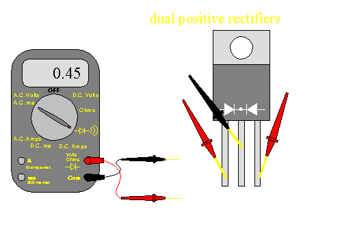
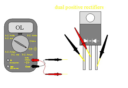
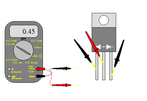
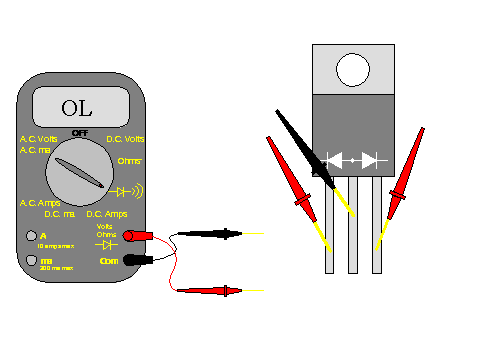
Checking Dual Diodes/Rectifiers
These first 2 diagram show how to check the dual positive rectifiers (diodes) and the associated meter readings. The windings of the transformer would go to the two outside legs and the center terminal would go to the positive rail capacitor.
The next 2 diagram show how to check the dual negative rectifiers (diodes) and the associated meter readings. The windings of the transformer would go to the two outside legs and the center terminal would go to the negative rail capacitor.
Notes:
If any combinations of meter leads to component terminals on any of the aforementioned devices reads less than 0.2 volts with the meter on diode-check and the component out of the circuit, the device is likely defective. There should be no connections on any of the devices that will cause the meter to read 0.00 while on diode check. The only exception will be the rectifiers. The outside legs of the dual rectifiers will typically be directly connected through the transformer windings. This will make it appear to be a dead short but you're simply reading the secondary windings on the transformer which have very low resistance.
Remember to test the FETs in the proper order.
All of the devices must be removed from the circuit to have definitive test results but it's generally possible to find components with an internal dead short while the component is still in the circuit. Many times, there are multiple, parallel-connected components. When one of these components fails, it often makes the ones in parallel with it appear to be shorted also. When this happens, you have to remove all of the ones that appear shorted to find the one that's actually shorted. If these are output transistors, you can sometimes reinstall the good transistors to see if there are other faults. When one of a parallel group of transistors has failed, you have to replace the failed one and all that were connected in parallel with it with matching transistors. You don't have to do any testing to match transistors. Simply having them from the same production group (will have the same production code etched into the faces of the transistors) is close enough for virtually every circuit.
This site was started for pages/information that didn't fit well on my other sites. It includes topics from backing up computer files to small engine repair to 3D graphics software to basic information on diabetes.
This site introduces you to macro photography. Macro photography is nothing more than the photography of small objects. It can take quite a while to understand the limitations associated with this type of photography. Without help, people will struggle to get good images. Understanding what's possible and what's not possible makes the task much easier. If you need to photograph relatively small objects (6" in height/width down to a few thousandths of an inch), this site will help.
If you're interested in air rifles, this site will introduce you to the types of rifles available and many of the things you'll need to know to shoot accurately. It also touches on field target competition. There are links to some of the better sites and forums as well as a collection of interactive demos.
This site helps anyone new to computers and anyone with a basic understanding of computers with a desire to learn more about the internal components of a computer. If you have a computer that you'd like to upgrade but don't know where to start, this is a good site for you.
This site is for those who want to begin racing karts but don't fully understand how the various parts work. It's mostly interactive demos that show how the various parts of the kart work.
Click HERE to visit a friend's new car audio tech site.